The ports of a VHDL entity are the system inputs and outputs. Physical connection of the system ports to the outside world are made through pins on the FPGA package. In Xilinx Vivado, the mapping from ports to pins is specified by a constraints file that is processed along with the VHDL source files.
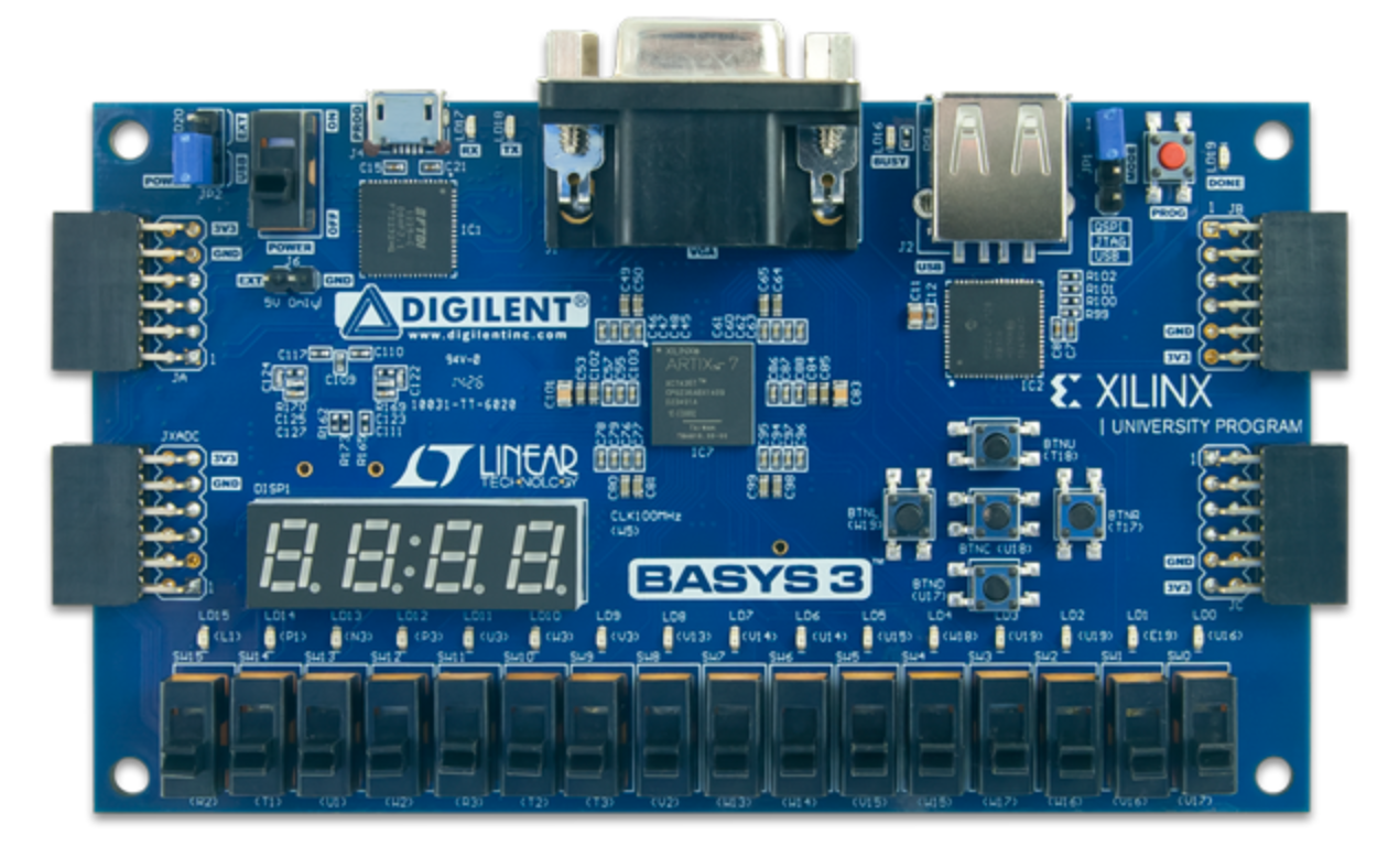
In this class, the FPGA is mounted on a development board with switches, LEDs, and a variety of input/output connections, Figure 11.2.1.
Figure11.2.1.Top view of the Digilent Basys3 development board. For a more detailed view, see Figure 1 and Table 1 of the reference manual, [3].
Checkpoint11.2.2.How big is our FPGA?
According to the Basys3 documentation, what FPGA is used on the board? Then use the Xilinx website 1
to find out how many LUTs and flip-flops this FPGA possesses.
Each switch, LED, etc, on the development board is wired to a pin on the FPGA, as described in the documentation [3]. These connections are listed in a corresponding constraints file, available for download 2
Listing11.2.3.Three entries from the constraints (XDC) file for the Basys3 board, showing mappings from the FPGA to the board clock and two slide switches. The third entry is commented out by the # character.
The XDC file is not written in VHDL, and consequently the entries have non-VHDL syntax. In particular, port names are case-sensitive (“clk” and “CLK” are read as different names). The Basys3 board’s clock signal is supplied by a chip that is wired to pin W5 on the FPGA, as can be confirmed by referring to the Basys3 schematic diagram, [4]. The first entry in the XDC file, set_property PACKAGE_PIN W5 [get_ports clk], indicates that pin W5 will be routed inside the FPGA to an entity port called “clk”. In this way the board clock signal is connected through pin W5 to the clock input of your design. If the clock port of your entity is named something other than clk, edit this line and the following two lines to use the correct name, taking care to write the name with the same case in the entity and the XDC file. (The two lines following can be ignored for now, except to note that the name of the clock port must be the same in all three lines.)
Likewise, the second entry indicates that one of the sixteen slide switches on the board is wired to FPGA pin V17. Again, look at the schematic [4] to see how this is done. To use this switch as an input to your design, replace the default name sw[0] with the name of the appropriate port in your design’s entity. This port name must be used in both lines of the entry, and the case must match the case in your entity.
Unused lines in the downloaded XDC file are preceded by the XDC comment character, #, as shown in the third entry.