Draw the logic diagram for a shift register that shifts left, rather than right.
Section 17.1 Shift register logic
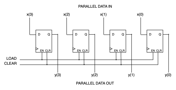
As we have seen, a register is a set of flip-flops for holding a binary vector. The flip-flops in the register frequently share common enable and reset controls, as shown in Figure 17.1.1.
A different kind of register is created by chaining flip-flops together, as shown in Figure 17.1.2.

When SHIFT is asserted, the flip-flops are all enabled to load. On the rising clock edge, then, the SERIAL DATA IN signal is loaded into the first flip-flop (y(0)), the contents of the first flip-flop are loaded into the second flip-flop (y(1)), etc. If the register holds "1011" and the SERIAL input is ’1’ prior to the clock edge, after the clock edge the register will hold "1101". If SERIAL is changed to ’0’, after the next clock edge the register will hold "0110". If SHIFT is deasserted, the register will continue to hold "0110" after the next clock edge. A register with this structure is called a shift register.
Checkpoint 17.1.3. A left-shifting register.
The register in Figure 17.1.2 has serial input and parallel output. It is also possible to have a register that loads in parallel and outputs serially. This is shown in Figure 17.1.4. This is a bare-bones version of the parallel-to-serial register that is always shifting except when it is being loaded. An additional input can be added to enable or disable the shifting.
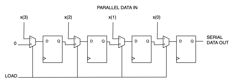
Checkpoint 17.1.5. Parallel-to-serial shift register.
A more flexible version of the parallel-to-serial shift register includes an input to control whether the register shifts or not. Draw the logic diagram for a register with both LOAD and SHIFT controls. LOAD has priority over SHIFT. If LOAD and SHIFT are both 0, the register holds its contents.
Hint.
Expand the multiplexers to have more inputs.