Section 19.2 SPI protocol
The SPI bus is diagrammed in Figure 19.2.1. The bus is designed to have one master device that controls the communication, and one or more peripheral devices. The single peripheral setup is most commonly encountered in this course.
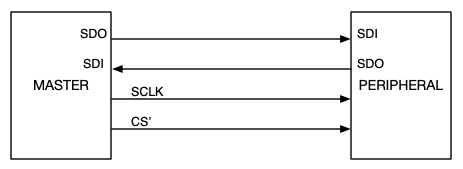
Four wires are defined between the master device and the peripheral device. Some peripherals are receive-only (e.g., digital-to-analog converters) and some are send-only (e.g., analog-to-digital converters). These will have both timing lines but only one data line. The designations in the figure for the SPI bus signals are SCLK, CS’, SDO, and SDI. Many variations exist, however (e.g., this list in a Wikipedia article).
1
en.wikipedia.org/wiki/Serial_Peripheral_Interface#InterfaceThe master initiates a SPI bus transaction by asserting the CS’ signal (LOW); it then holds it LOW for the duration of the transaction. One bit of data is sent (SDO) or received (SDI) in each SCLK cycle until the full packet (e.g., 16 bits) has been moved. The master concludes the transaction by releasing CS’. Each device has only one data (shift) register. When a peripheral device has both SDI and SDO ports, the received data is shifted into the data register as the transmitted data is shifted out of the same register.
This is straightforward enough, but the devil is in the details. Referring to Figure 19.2.2, the serial clock and the data streams are permitted by the SPI bus definition to have four possible timing relationships. The first SCLK edge following the CS’ transition from HIGH to LOW is called the “leading edge” (marked by a red line in the figure), and the opposite edge is called the “trailing edge” (marked by a blue line). The leading edge may either be rising (“positive polarity”, denoted CPOL=0) or falling (“negative polarity”, CPOL=1). Data bits are transmitted, or launched, on one SCLK edge and received, or captured, on the opposite edge. And, there are two possibilities for this: launch on the leading edge and capture on the trailing edge (CPHA=1), or vice versa (CPHA=0).
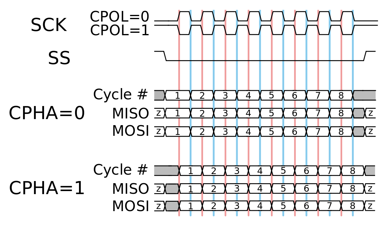
Timing diagram
The good news is that a particular peripheral device will implement only one of these four possibilities, and it will be documented in the device’s data sheet. An example is the timing diagram for the ADCS7476 analog-to-digital converter [10], below.
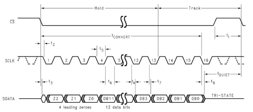
Timing diagram
Following the assertion of CS’ on the falling edge of the serial clock (SCLK), the serializing register inside the ADCS7476 shifts, launching a data bit onto the SDATA (SDO) line. On the next rising edge of SCLK, the deserializing register inside the master shifts, capturing the data bit. According to the timing diagram and the data sheet [10], the received data will be valid (clearly ’1’ or ’0’) and safe to capture no later than \(t_4=20\)ns after the falling edge. The maximum SCLK frequency is specified to be 20MHz (50ns period). Thus, the data is guaranteed to be valid for at least 5ns before the rising edge captures it.