In this section we’re going to see how to implement a prototype, or experimental version, of a logic circuit with integrated circuit logic gates on a solderless breadboard. This method is no longer used for industrial logic prototyping, but the technique is still important for other kinds of electronic experimentation and worth mastering.
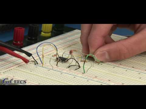
Watch the video from U.C. Berkeley to learn about how solderless breadboards work
The steps for converting a logic diagram to a prototype are:
Plan: Select components and prepare your logic diagram for hardware implementation.
Place: Plug the components into the breadboard, leaving room for wiring between them.
Route: Connect wires from pin to pin on the components.
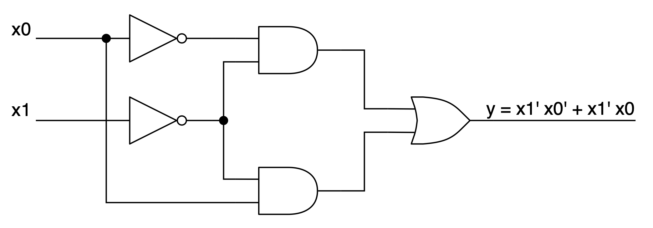
We illustrate the procedure using the earlier “\(x \lt 2\)” circuit, Figure 1.6.1,
Logic diagram with AND, OR, and NOT gate symbols wired together.
Figure1.6.1.\(x \lt 2\) circuit. The output \(y\) is TRUE when the input \((x_1, x_0)\) is less than 2
The first planning step is to select the necessary integrated circuits. A little browsing of a parts catalog (such as this list on Wikipedia 1
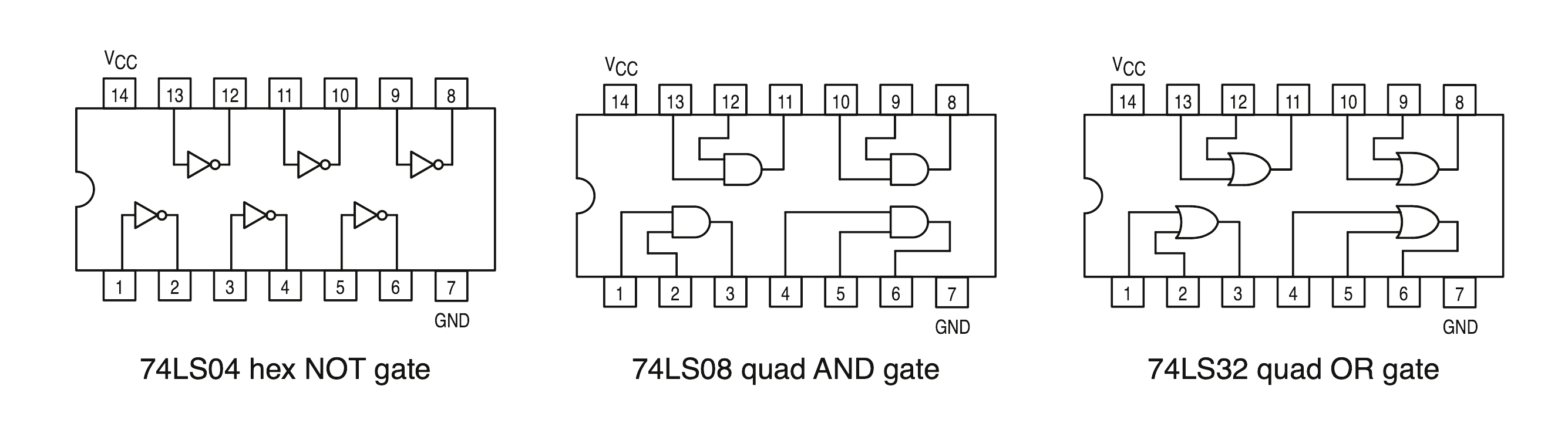
Package outlines for three integrated circuits, showing how pins are connected to logic gates inside.
Figure1.6.2.Package outlines for three integrated circuits containing (left to right), NOT, AND, and OR circuits.
Referring to Figure 1.6.2, here is how to read the part numbers:
The final digits, “04”, “08”, “32”, uniquely identify the circuits as “hex NOT gate”, “quad two-input AND gate”, and “quad two-input OR gate”, respectively.
The “LS” denotes a particular type of transistor used to make the logic circuits. There are several other types with different real-world characteristics such as speed and power consumption, but regardless of the technology, a ’08 part is a quad AND gate. The LS logic family was once quite common and popular for undemanding applications.
Finally, the “74” denotes commercial-grade components, as distinguished from the more rugged military-grade components, whose numbers begin with “54”.
As you hold an integrated circuit (IC) in your fingertips so you can see the labeling on top, rotate it so that there is either a notch at the left end or a dot at the lower left corner. This orients the IC so that Pin 1 is at the lower left corner. As shown in the diagrams above, the pin numbers increase from left to right along the bottom edge of the IC and then from right to left along the upper edge. The first and last pins are above each other at the left end of the IC; in all three of these, that’s Pin 1 and Pin 14.
The power and ground pins (labeled VCC and GND, respectively, on the diagrams above) are how the logic gates inside the integrated circuit are supplied with electric current so they can function. They are not shown on logic diagrams, but must not be neglected when you wire up a circuit!
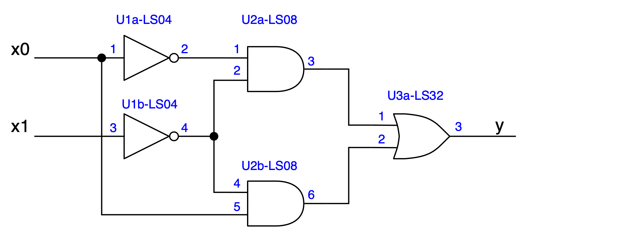
The next planning step is to annotate the logic diagram, Figure 1.6.3:
Annotated logic diagram
Figure1.6.3.\(x \lt 2\) circuit, annotated with reference designators and pin numbers.
Each logic gate is identified by a unique reference designator, or REFDES; here, U1a and U1b denote two of the six NOT gates in the LS04, U2a and U2b denote two of the four AND gates in the LS08, and U3a denotes one of the four OR gates in the LS32. The designation of a gate as “a”, “b”, etc, is arbitrary, but usually the letters are assigned as you go around the chip in a counter-clockwise direction from pin 1 to pin 14 (or whatever the last pin is). The gate inputs and outputs are labeled on the diagram by their respective pin numbers on the integrated circuit.
Each wire (or branching tree of wires) from one input port or gate output to one or more output ports or other gate inputs is called a net. From the annotated logic diagram you may optionally create a table called a netlist that shows all the nets in the circuit, Figure 1.6.4. You should compare the netlist with the annotated logic diagram to make sure you understand how the two fit together.
Source (from)
Destination (to)
Power and ground nets
Vcc
U1-14, U2-14, U3-14
GND
U1-7, U2-7, U3-7
Input and output nets
Input x0
U1-1, U2-5
Input x1
U1-3
U3-3
Output y
Signal nets
U1-2
U2-1
U1-4
U2-2, U2-4
U2-3
U3-1
U2-6
U3-2
Figure1.6.4.Netlist for the \(x \lt 2\) circuit.
In the netlist, “U\(m\)-\(n\)” denotes pin \(n\) of integrated circuit U\(m\text{.}\)
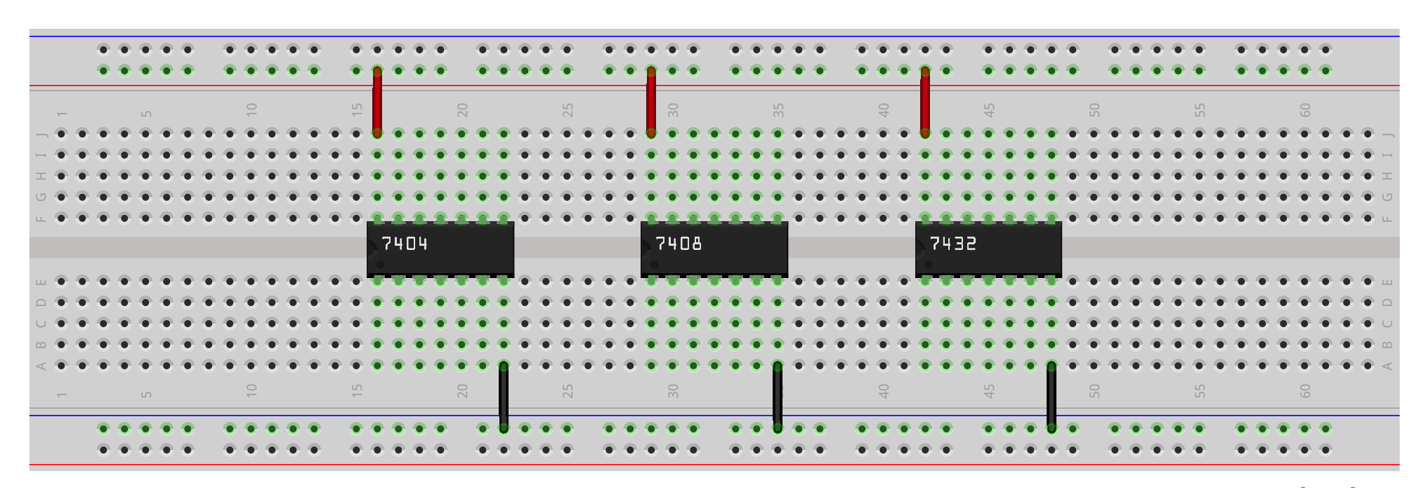
The placing step consists of arranging the integrated circuits on the breadboard to make wiring as convenient as possible. Here, since the signals move cleanly from U1 to U2 to U3 in the logic diagram, it makes sense to arrange the LS04, LS08, and LS32 in order from left to right on the breadboard, Figure 1.6.5. The three ICs are oriented identically, with Pin 1 at the lower left corner. Power and ground wires have also been installed. Power is always wired with red wire and ground is always wired with black wire. Red and black are never used for anything other than power and ground.
Figure1.6.5.Integrated circuits placed on a solderless breadboard, with power and groud wired.
In the routing step, the connections tabulated in the netlist are made. We have already seen the power and ground connections. They should be short and low to the board so they are out of the way and cannot accidentally be pulled loose.
Following the power and ground, the input and output connections are made. It is unlikely that these will need to be changed once the circuit is wired, so they should also be kept low to the surface of the board. Consider using colors of wire to identify inputs and outputs (but don’t use red or black!).
Finally, route the signal nets between the gate inputs and outputs. These really define the logic function implemented by the circuit, and are the most likely to be changed as you debug the circuit and correct logic errors or wiring errors. It’s OK for these wires to have a little extra slack for convenience.
The routed prototype is shown in Figure 1.6.6. Compare the breadboard with the netlist to verify the wiring. Can you identify which wire corresponds to each input, and which wire is the output?
Diagram of a solderless breadboard with three integrated circuits and wiring.
Figure1.6.6.The breadboarded \(x \lt 2\) circuit with logic signals routed.
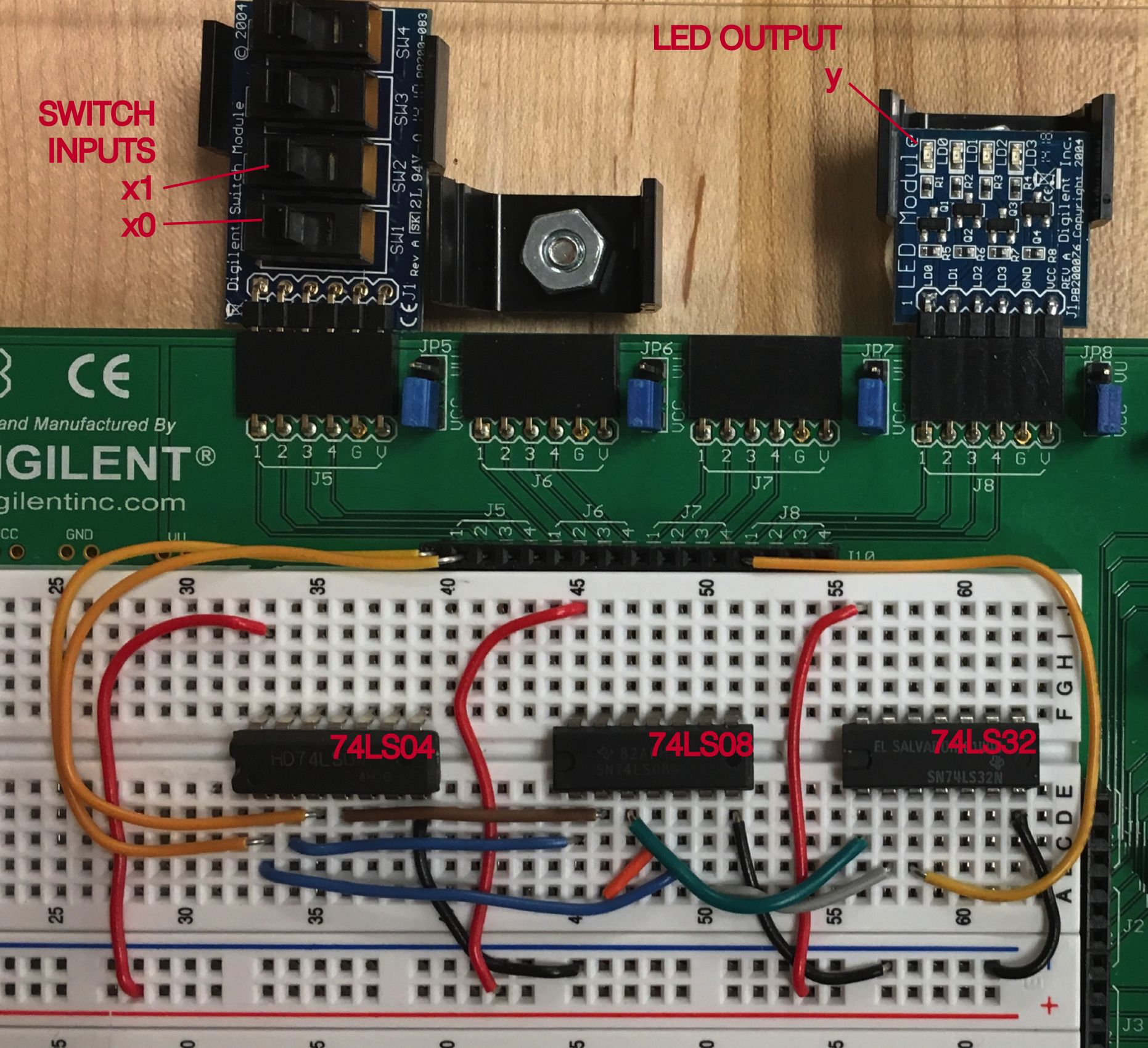
An actual breadboard, wired in the lab, is shown in Figure 1.6.7. Compare the photograph with the diagram in Figure 1.6.6.
Photograph of circuit wired on solderless breadboard.
Figure1.6.7.The \(x \lt 2\) circuit prototyped on a solderless breadboard.
The final step in developing a prototype is testing: Does the circuit behave as desired? For the circuit in Figure 1.6.7, switches connect the inputs \(x_0\) and \(x_1\) to power (1) or ground (0). The output \(y\) is wired to a light-emitting diode (LED). Testing consists simply of applying the inputs \(00, 01, 10, 11\) sequentially via the switches and observing whether the LED is appropriately on or off.
There are ways to build a digital system other than prototyping on a solderless breadboard, but they all follow the same basic steps introduced in this chapter. Make sure to stick to this process in lab and in your designs for this course.
Capture (Section 1.3 and Section 1.4): Expressing the desired system behavior, e.g., in a truth table and logic equations.
Synthesis (Section 1.5 and Section 1.6): Translating the captured design to a logic diagram and/or a list of required components and a netlist.
Implementation (Section 1.6): Placing components in a physical layout and routing the connections specified in the netlist.
Testing: Verifying that the prototype functions as intended.
Practice.
For each of the logic diagrams you developed in the last section, select the necessary 7400-series integrated circuits, annotate the logic diagram, and write a netlist.
Coming up in the next chapter, we will learn about the electronics inside logic gates, and some real-world properties of these gates like their speed, size, and power consumption. We will then learn some techniques for simplifying logic equations so that implemented designs are faster, smaller, and consume less power, all of which are highly desirable in a practical system.