Section 11.1 Programmable logic
VHDL modeling enables the capture of a digital system’s behavior and also the verification of a design through simulation, before the design is committed to hardware. EDA tools also perform logic synthesis and implementation, moving from the VHDL model to a hardware prototype.
The hardware prototypes we saw in Section 1.6 used so-called small-scale integration (SSI) and medium-scale integration (MSI) technology: individual packages containing the familiar combinational logic (gates, multiplexers, decoders, adders, etc) and memory elements (flip-flops, registers). Modern integrated systems put orders of magnitude more capability into a single small package. This is true not just of finished systems (e.g., microcontrollers), but also prototypes. Programmable logic is the name given to devices containing a multitude of combinational and storage elements, with interconnects that can be configured and reconfigured by the user, enabling the flexible creation, testing, and revising of large prototypes.
The dominant programmable logic device in use today is the field programmable gate array (FPGA). The basic structure of an FPGA is an array of thousands of configurable logic blocks (CLBs), each of which contains one or more logic slices, which are pairings of a small block of combinational logic with a flip-flop, Figure 11.1.1.
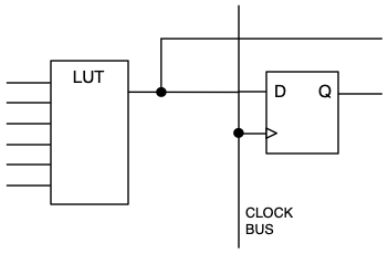
The combinational logic in the slice is not constructed from gates, but is itself a small block of programmable memory called a lookup table (LUT) Figure 11.1.2.
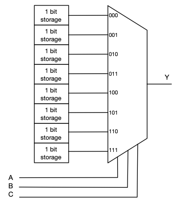
As shown in the figure, a three-input LUT, storing \(2^3=8\) bits, can hold the truth table for any logical function of three inputs, \(Y = f(A, B, C)\text{.}\) The appropriate 1s and 0s are stored in the LUT when the FPGA is configured (programmed). The model shown in the figure is a simplification: LUTs used in contemporary FPGAs have four or six inputs. The LUT output may be routed either to a flip-flop, for storage, or to an input of another LUT, to make a more complex logical function, as shown in Figure 11.1.1.
The array of CLBs is enmeshed in a network of wires resembling the traffic lanes in a city. Signals are routed from CLB to CLB along these wires with switches that are set when the FPGA is configured. The clock lines for the flip-flops have their own special paths designed so that, as much as possible, the clock arrives at each flip-flop at the same time. Special circuits, called buffers, interface the internal wiring to pins on the FPGA package and the outside world.