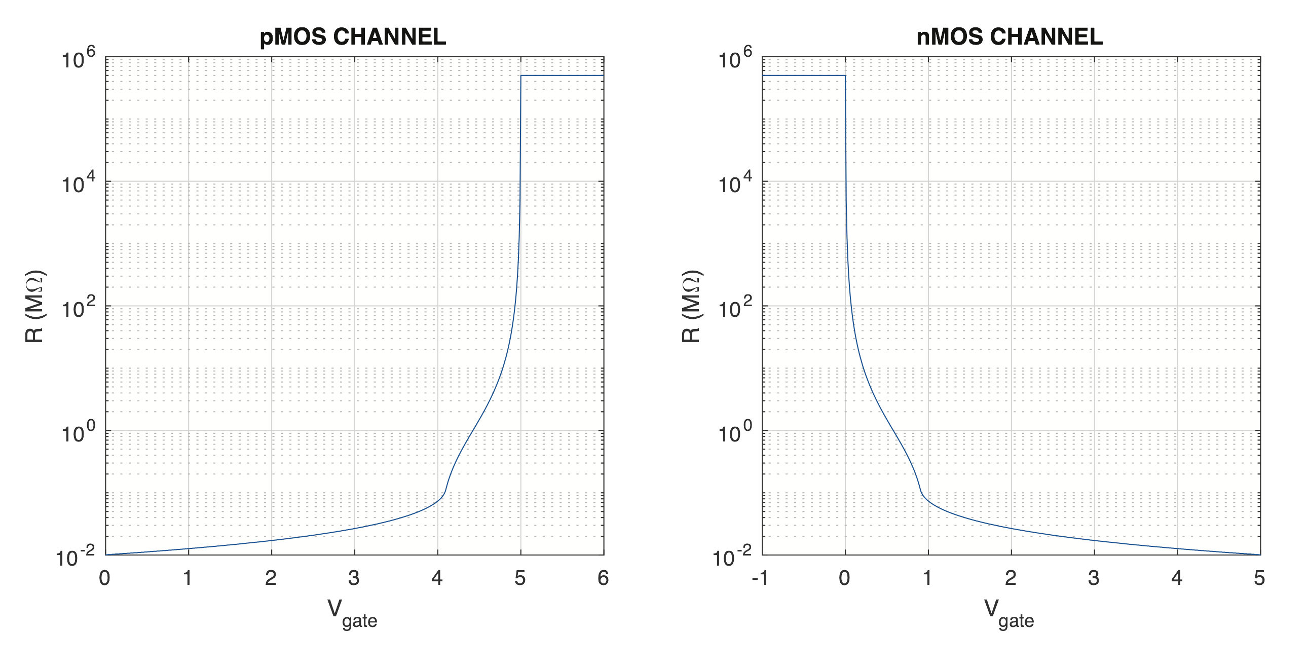
Review Figure 2.3.2, Figure 2.3.4, and Figure 2.3.5, summarizing for yourself how the nMOS and pMOS transistor circuits work.
Section 2.3 Electronic switches (transistors)
You have observed that the output of the voltage divider circuit can be controlled by changing the resistances. With reference to Figure 2.3.1, below, the voltage divider equation derived earlier says
\begin{gather*}
V_\text{out} = V \times \frac{R_2}{R_1 + R_2}.
\end{gather*}
Now, two extreme cases are of primary interest for logic design.
- \(R_2 \gg R_1\text{.}\) In particular, if \(R_1 \approx 0\) and \(R_2 \to \infty\text{,}\) the output "sees" a low resistance path to the supply voltage, and the output voltage is \(V\text{,}\) or HIGH.
- \(R_2 \ll R_1\text{.}\) In particular, if \(R_1 \to \infty\) and \(R_2 \approx 0\text{,}\) the output sees a low resistance path to ground, and the output voltage is 0, or LOW.
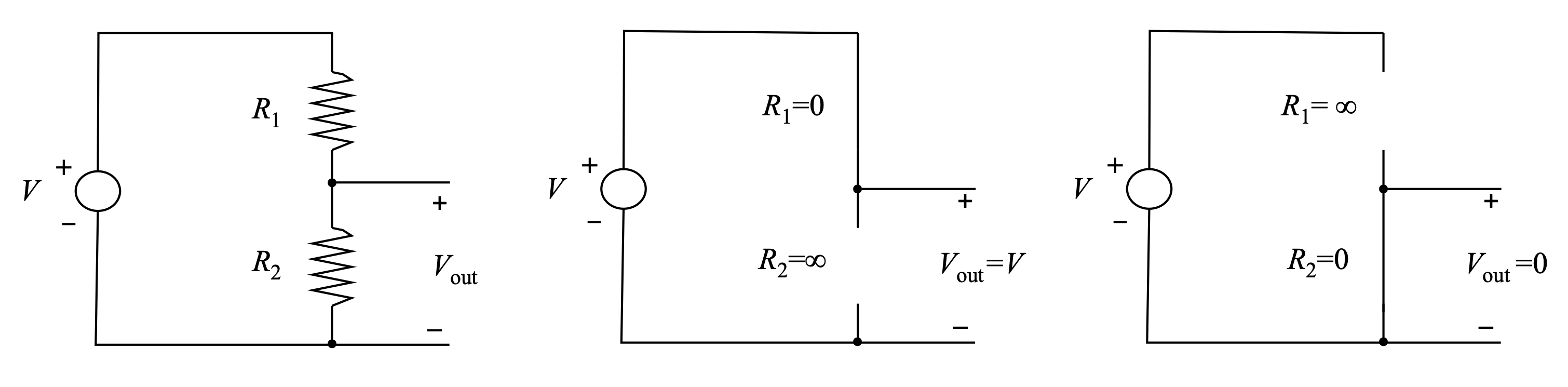
These extreme cases of resistance are identical to the function of a switch. A closed switch has very low resistance to current flow, and an open switch has infinite resistance (Figure 2.3.2). (Unlike a door, a closed switch allows current to flow.)
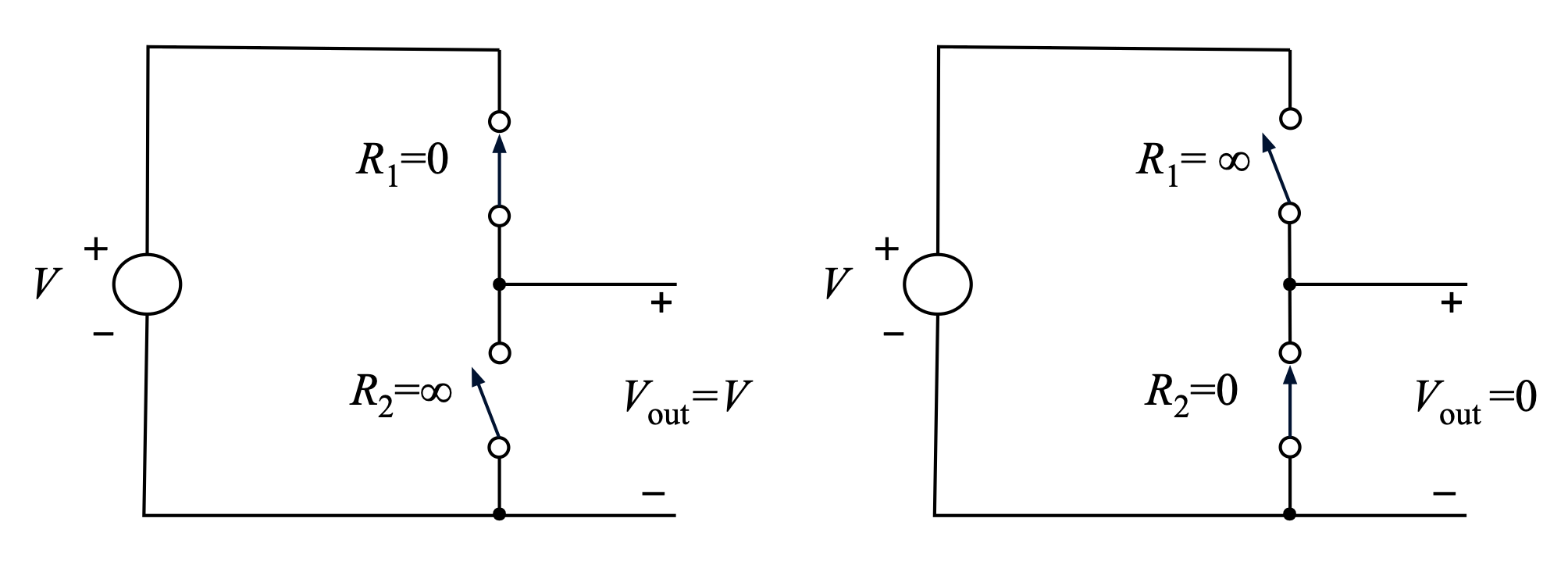
The key step is to make the resistances/switches controllable electrically by HIGH and LOW input voltages. These electrically-controlled resistors/switches are called transistors. The particular transistors we will use are fabricated using so-called MOS ("metal-oxide-semiconductor") technology. For our purposes we can skip over the physics of how they work and simply regard them as voltage controlled resistors or, even simpler, as voltage controlled switches.
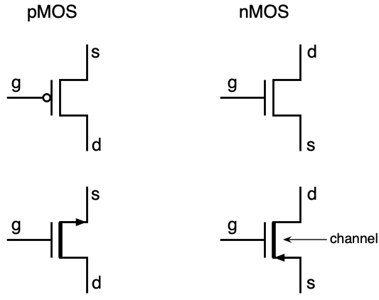
There are two types of MOS transistor, called pMOS and nMOS. Both have three terminals, called the gate, source, and drain. They are distinguished in a circuit diagram by slightly different symbols, shown in Figure 2.3.3. The lower pair of symbols has the advantage of identifying the source by an arrow, and distinguishing pMOS from nMOS by the direction of the arrow. However, the upper pair of symbols is more common in digital design and will be used here.
The operation of the two kinds of transistors can be observed by inserting them in place of one of the resistors in a voltage divider circuit, Figure 2.3.4. The curves in the figure are produced by simulating the circuits with the LTSpice software, a free download from Analog Devices [8]. These simulated voltage curves correctly illustrate general behavior. The physical parameters of a transistor’s design can be varied to affect the detailed shape of the curve for particular applications.
- When the gate voltage of the pMOS transistor is at or above the source voltage, the resistance of the channel is very high, approximately infinite. When the gate is lower than the source, the channel resistance decreases as the gate voltage decreases, to a very small value when the gate voltage is near zero. Consequently, the output voltage of the circuit rises as the gate voltage decreases. We say that the pMOS transistor "pulls the output up".
- When the gate voltage of the nMOS transistor is at or below the source voltage, the resistance of the channel is very high, approximately infinite. When the gate is higher than the source, the resistance decreases as the gate voltage increases, to a very small value when the gate voltage is near the supply voltage. Consequently, the output voltage of the circuit decreases as the gate voltage increases. We say that the nMOS transistor "pulls the output down".
The gate voltage, by controlling the resistance of the transistor channel, switches the output voltage between a HIGH and LOW level, with a narrow transition region.
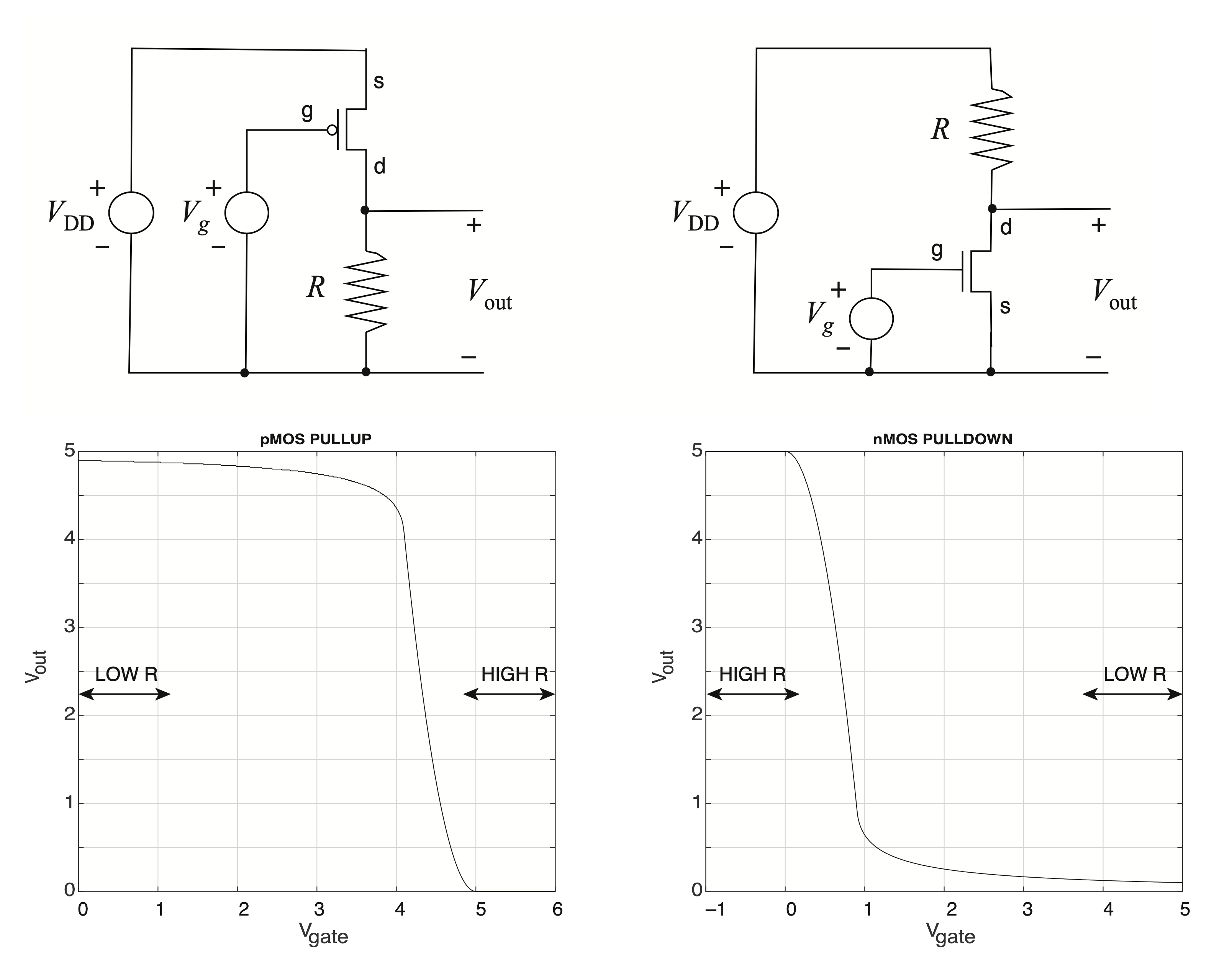
The pMOS and nMOS transistors are always used as shown in Figure 2.3.4, the pMOS transistor with its source connected to the supply voltage \(V_{DD}\text{,}\) and the nMOS transistor with its source connected toward ground. The physical reasons for this are beyond the scope of this course, but are explained in many electronics texts.
Another way to visualize the operation of the two transistors is to compute and plot the resistance of the channel as a function of the gate voltage. This is shown in Figure 2.3.5.
- The resistance of the pMOS transistor is low when the gate voltage is LOW, and very high when the gate voltage is HIGH.
- Conversely, the resistance of the nMOS transistor is very high when the gate voltage is LOW, and low when the gate voltage is HIGH.
When the transistor has an approximately infinite resistance, it is like an open (non-conducting) switch, and in comparison, when it has a low resistance, it is like a closed (conducting) switch. Thus, we can see how the transistors fulfill the roles of approximately ideal zero and infinite resistances illustrated earlier, in Figure 2.3.1.