Look again at Figure 2.3.4. In both the pMOS and nMOS circuits, when the input voltage, \(V_{gate}\text{,}\) is LOW, the output voltage is HIGH, and when the input is HIGH, the output is LOW. Either circuit could be used to implement a NOT gate. Indeed, for many years logic circuits were fabricated solely from nMOS transistors. Today, the dominant technology is complementary MOS, or CMOS, which uses both nMOS and pMOS transistors. A CMOS NOT gate is shown in Figure 2.4.1, together with its voltage curve, obtained by LTspice simulation.
Figure2.4.1.The CMOS inverter (left) and its simulated voltage characteristic curve (right).
The CMOS inverter consists of a pMOS transistor stacked on top of an nMOS transistor. When the input voltage is LOW, the pMOS transistor is ON and the nMOS transistor is OFF. The output is connected via the low-resistance pMOS transistor to \(V_{DD}\text{,}\) creating a HIGH output. When the input voltage is HIGH, the pMOS transistor is OFF and the nMOS transistor is ON, and the output is connected via the low-resistance nMOS transistor to ground, creating a LOW output.
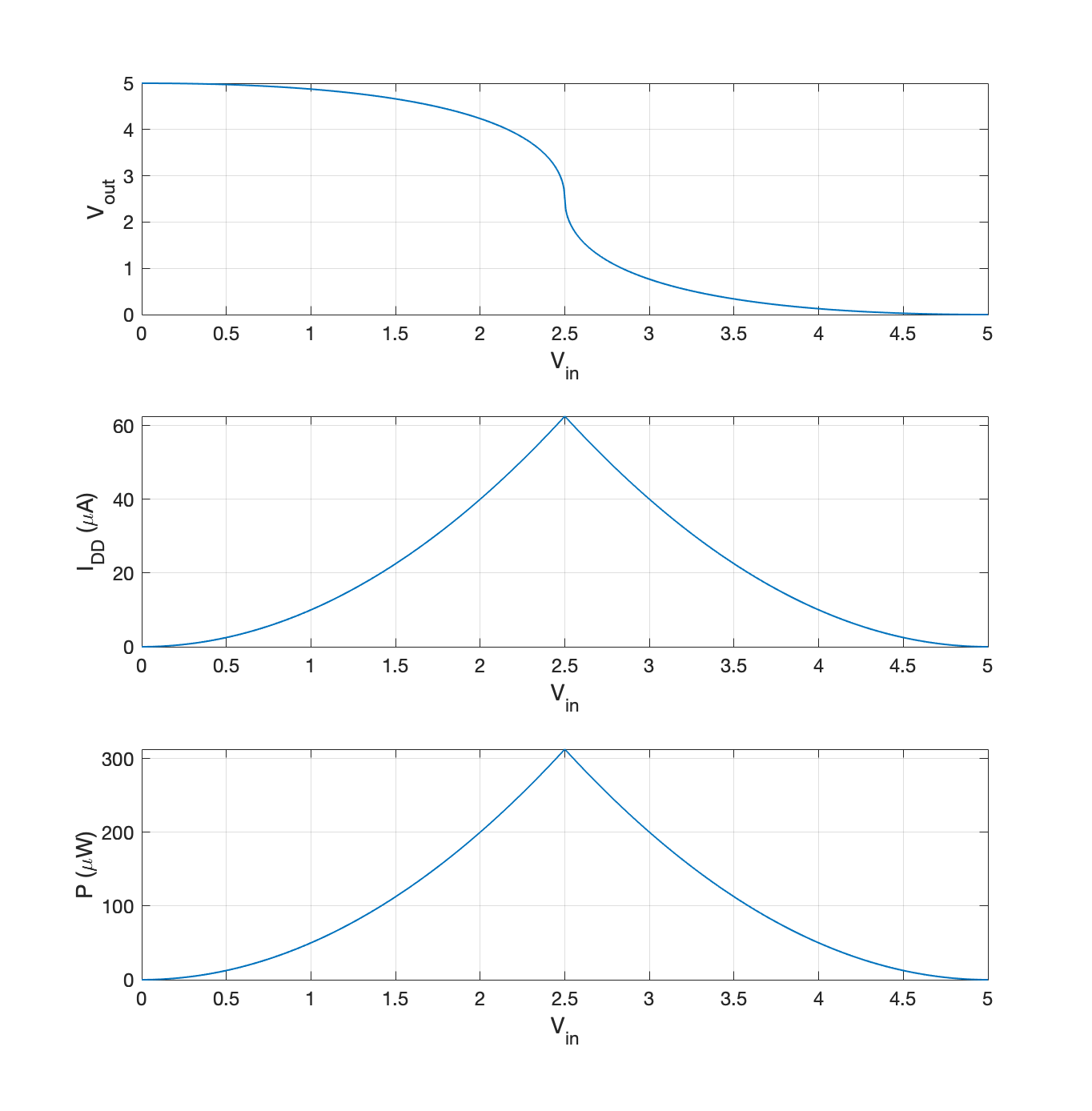
As the input increases from LOW to HIGH, there is a point in the middle where the output rapidly switches from HIGH to LOW. In practice, input voltages around this transition are avoided. Figure 2.4.2, below, shows why. The current, \(I_{DD}\text{,}\) that flows from power to ground through the two transistors peaks midway between the LOW and HIGH extremes of the input voltage \(V_{in}\text{.}\) When the input is LOW, the nMOS transistor is off and little current flows. When the input is HIGH, the pMOS transistor is off and, again, little current flows. But in the middle between LOW and HIGH, both transistors are partially on and a considerable amount of current is able to flow. The bottom graph in the figure plots the power consumption, \(P=V_{DD}I_{DD}\text{,}\) and shows that power consumption is also maximized between the extreme LOW and HIGH input voltages. To minimize power consumption, then, the circuit is operated so that the transistors function as switches, snapping rapidly between ON and OFF, spending negligible time in the mid-range, high power zone.
Figure2.4.2.(Top) Output voltage of the simulated CMOS inverter. (Middle) The current flowing through the two transistors, from power to ground, is lowest at the extremes of \(V_{in}\text{.}\) (Bottom) The power dissipated in the transistors is lowest at the extremes of \(V_{in}\text{.}\)
CMOS AND and OR gates.
We can build out from the CMOS inverter circuit to construct AND and OR gates, but the path will turn out to be rather indirect. For an AND gate, we want two HIGH inputs to result in a HIGH output. However, pMOS transistors, which connect the output to power, are only ON when their gate inputs are LOW. Likewise, for an OR gate, we want two LOW inputs to result in a LOW output, but nMOS transistors, which connect the output to ground, are only ON when their gate inputs are HIGH. The transistors appear to be backwards from what we need them to be.
On the other hand, we can easily construct inverting AND and OR gates, known as NAND and NOR.
Checkpoint2.4.3.
Two other interesting logical operations are NAND (NOT AND) and NOR (NOT OR). Write truth tables for these two operations.
Answer.
\(a\)
\(b\)
\(a\) NAND \(b\)
0
0
1
0
1
1
1
0
1
1
1
0
\(a\)
\(b\)
\(a\) NOR \(b\)
0
0
1
0
1
0
1
0
0
1
1
0
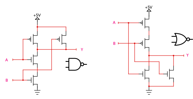
Opposite the definition of the AND gate, the NAND gate has a LOW output when both of its inputs are HIGH, and a HIGH output when either of its inputs is LOW. This fits with the way that pMOS and nMOS transistors work. Likewise, opposite the definition of the OR gate, the NOR gate has a LOW output when either of its inputs is high, and a HIGH output when both inputs are LOW. Again, this matches the behavior of the pMOS and nMOS transistors. The NAND and NOR circuits are shown, with their logic symbols, in Figure 2.4.4, below.
Figure2.4.4.The CMOS NAND (left) and NOR (right) gates, symbols and circuits.
In the NAND circuit, the two nMOS transistors are in series. When the inputs are both HIGH, both of the nMOS transistors are ON, providing a low-resistance path from the output to ground, as desired. The two pMOS transistors are off. When either input is LOW, one of the pMOS transistors will be ON, providing a low-resistance path from the output to power, and one of the nMOS transistors will be OFF, blocking the path from output to ground. Consequently, the output is HIGH. Apply the same reasoning to the NOR circuit, and convince yourself that it works as it is supposed to.
Checkpoint2.4.5.
To review, explain, transistor-by-transistor, how the NAND and NOR circuits work.
A NAND gate with more than two inputs is constructed by adding one pMOS-nMOS pair for each additional input. The pMOS transistor is added in parallel with the existing pMOS transistors between the output and power, and the nMOS transistor is added in series with the existing nMOS transistors between the output and ground. Similarly, the NOR gate may be expanded by adding one pMOS-nMOS pair for each additional input.
Checkpoint2.4.6.
Draw a three-input NAND circuit and a three-input NOR circuit.
Answer.
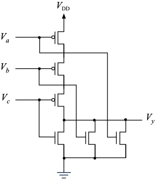
Figure2.4.7.Three-input CMOS NAND gate (left). Three-input CMOS NOR gate (right). When all three inputs are HIGH, the three nMOS transistors in the NAND are all ON, pulling the output LOW. When all three inputs are LOW, the three pMOS transistors in the NOR are all ON, pulling the output HIGH.
A true AND or OR gate is constructed by driving an inverter circuit with the output of a NAND or NOR gate, respectively. That is, an AND gate is a "NOT NAND" and an OR gate is a "NOT NOR".
Checkpoint2.4.8.
Draw the circuit for a two-input OR gate.
Answer.
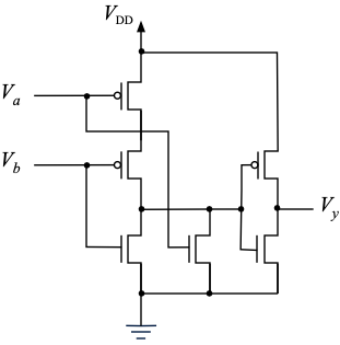
Figure2.4.9.Two-input CMOS OR gate is a NOR followed by a NOT.
Checkpoint2.4.10.
Count the transistors: Figure out a general expression for the number of transistors in an \(n\)-input NAND or NOR gate. How does this compare with the transistor count for an AND or OR gate with the same number of inputs?
Answer.
NAND or NOR: Two transistors per input, or \(2n\) transistors in all.
AND or OR: AND and OR are NAND and NOR, followed by inverters. Add two transistors for the inverter at the output, or \(2(n+1)\) transistors in all.
Logic families.
Since the introduction of digital integrated circuits in the 1960s, logic circuit designs have evolved, becoming smaller, faster, and more power-efficient. Today you are likely only to encounter logic families based on CMOS technology. An older technology, known as bipolar, or transistor-transistor logic (TTL), is still occasionally seen. We use a bipolar family denoted LSTTL in the early labs for this course, because bipolar devices are generally more durable for breadboarding by beginning students. Other important practical distinctions between CMOS and TTL will be made in the following sections. A broad spectrum of discrete integrated circuit logic families is described in the Texas Instruments Logic Guide [14].