Section 2.5 Electrical characteristics of logic circuits
Voltage.
Under normal operation, the inputs and outputs of a logic gate circuit are either LOW -- close to ground -- or HIGH -- close to the supply voltage. The valid ranges for LOW and HIGH inputs and outputs are specified by four parameters:
- A valid LOW input is required be less than a specified value denoted \(V_{IL}\) (voltage-in-low).
- valid HIGH input is required to be greater than a specified value, denoted \(V_{IH}\) (voltage-in-high).
- A valid LOW output is required to be less than a specified value denoted \(V_{OL}\) (voltage-out-low).
- A valid HIGH output is required to be greater than a specified value denoted \(V_{OH}\) (voltage-out-high).
The actual values of these parameters in a particular circuit depend on the physical design of the transistors, but are consistent across integrated circuits in the same family, e.g., the LS devices used in Section 1.6. The relevant portions of a 74LS00 (quad two-input NAND) datasheet [11], showing the input and output voltage limits, are shown in Figure 2.5.1, below. LSTTL devices operate with a nominal supply voltage (\(V_{CC}\)) of 5V. Certain CMOS logic devices may also operate from a 5V supply with compatible input and output voltage levels. Many other CMOS devices operate at lower supply voltages—3.3V or less—and are not TTL-compatible without special precautions being taken.
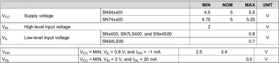
From the table in the figure, we read:
- \(V_{IL}=0.8\)V
- \(V_{IH}=2.0\)V
- \(V_{OH}\) is typically 3.4V, but could be as low as 2.5V.
- \(V_{OL}\) is no larger than 0.5V.
The minimum and maximum voltages are also known as the worst case values.
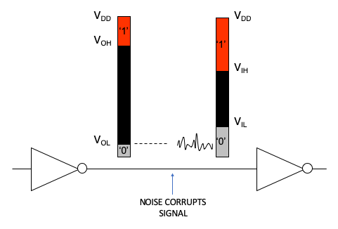
Usually, the output of one gate will be connected to drive the input of another gate. If the output is a valid LOW (less than 0.5V), it will certainly be low enough to satisfy the input requirement of the following gate (less than 0.8V). Likewise, if the output is HIGH (at least 2.5V), it will be certainly be high enough to satisfy the input requirement of the following gate (higher than 2.0V). It is always the case that \(V_{OL} \lt V_{IL}\) and \(V_{OH} \gt V_{OL}\) (Figure 2.5.2). The gaps between the output and input voltage specifications are called the noise margin of the circuit. With reference to the figure, even if some noise causes a LOW output to be slightly larger than 0.4V, it will still be recognized as a valid LOW by the following gate input. Similarly, a HIGH output corrupted by noise can still be high enough to be recognized as a valid HIGH by the following gate input.
Current.
In a typical circuit, the output of a logic gate drives another circuit or component, which is called a load. (Figure 2.5.3). All loads require current, and that current must be supplied by the driver. As shown in the figure, current may flow either direction between the driver and the load.
- When the driver is HIGH, current flows from the power supply, through the gate output, into the load and then to ground. The driver is said to source the load current.
- When the driver is LOW, current flows from the power supply, through the load into the gate output and then to ground. The driver is said to sink the load current.
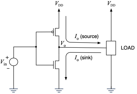
The amount of current a driver may source or sink is limited. Current flowing out of the gate passes through the channel of a pMOS transistor, which has a finite resistance even then the transistor is ON. By Ohm’s law, \(V = IR\text{,}\) there is a voltage drop across the transistor that increases as more current is drawn by the load. This voltage drop lowers \(V_{O}\text{,}\) and since \(V_{O}\) is guaranteed to be higher than \(V_{OH}\text{,}\) \(I_{O}\) must not exceed a certain maximum value. This maximum output current is denoted \(I_{OH}\) (current-out-high). Similarly, current flowing into the gate passes through the channel of the nMOS transistor, which also has a finite resistance when the transistor is ON. Increasing current increases the voltage drop across the nMOS channel, and since \(V_{O}\) is guaranteed to be lower than \(V_{OL}\text{,}\) there is also a limit to how much current may be sunk by the gate output. This value is denoted \(I_{OL}\) (current-out-low).
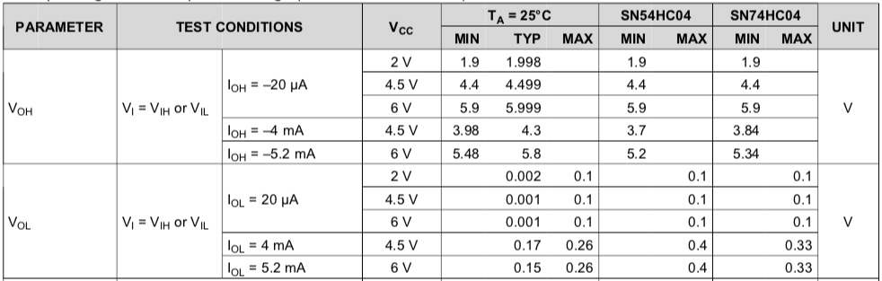
The datasheet for a typical HC-series device [13] is excerpted in Figure 2.5.4. According to the table in the figure, when the power supply is 4.5V, as much as 4 mA can be sourced or sinked, while the output voltage remains within acceptable HIGH and LOW limits.
In contrast, the TTL implementation of the same inverter function [13] has asymmetric output current specifications Figure 2.5.5: \(I_{OH}\) for the LS04 is 400\(\mu\)A, but \(I_{OL}\) is considerably larger, 8mA. (The physical reasons for the asymmetry are beyond the scope of this course; a good explanation may be found in the text by Wakerly [16], pp. 160-169.)
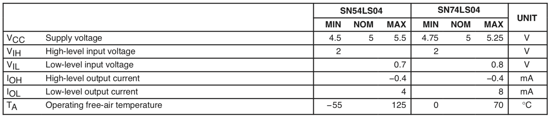
In both technologies, the output current of a logic gate is more than sufficient to drive the inputs of many logic gates at once; the input current requirements of logic gates are quite modest, on the order of nanoamps for CMOS devices and microapmps for TTL. A single LED requires more current, up to 10mA or more, and additional circuitry is required to go between a logic gate and a motor or large LED display. These design problems are explored in the lab.